
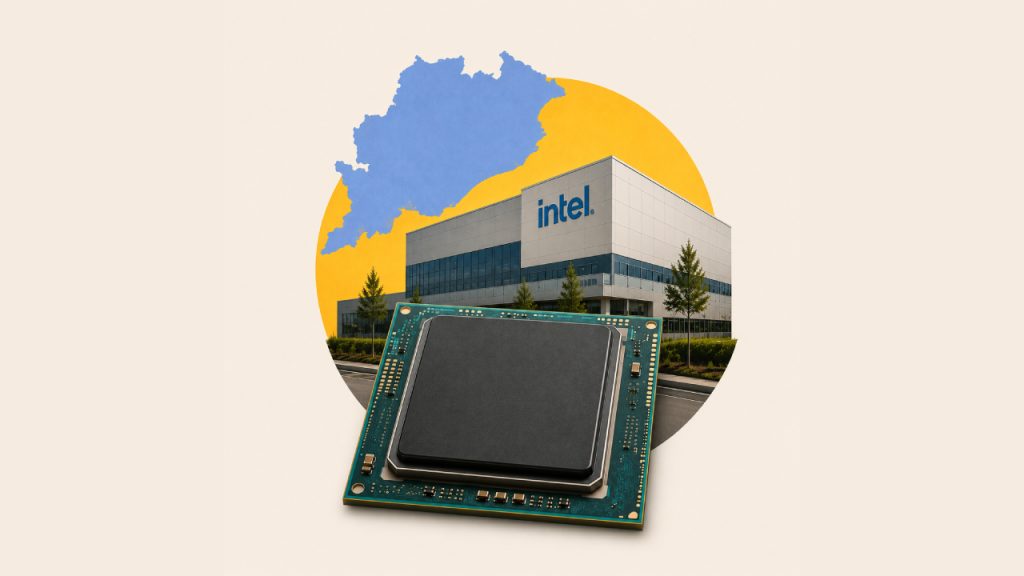
Bhubaneswar: India’s semiconductor ambitions received a major boost Friday after chip giant Intel Corporation signed a memorandum of understanding (MoU) with the Odisha government and 3D Glass Solutions (3DGS) to bring semiconductor substrate manufacturing technology to the country.
The proposed facility, likely to come up in the Bhubaneswar-Khurda region, involves an estimated investment of about $3.3 billion and is expected to create more than 1,800 direct high-skilled jobs.
Here is a closer look at what the project means and why it is important.
What exactly has been announced?
The Odisha government, Intel and 3DGS have signed an MoU to establish a semiconductor substrate manufacturing ecosystem in India.
The agreement was signed in the presence of Union Electronics and IT Minister Ashwini Vaishnaw, Chief Minister of Odisha Mohan Charan Majhi and Intel CEO Lip-Bu Tan.
The project will focus on manufacturing advanced semiconductor substrates, including glass core substrates and high-density interconnect substrates.
What is a semiconductor substrate?
A semiconductor substrate is the base layer on which electronic circuits and chip components are built.
It acts like the foundation of a building. The tiny transistors and electrical connections inside a semiconductor chip are constructed on top of this layer.
Substrates are essential for connecting chips to electronic devices and ensuring efficient power supply, heat management and signal transmission.
Why is this project significant for India?
The project is important for several reasons:
First major Intel-linked manufacturing engagement in India: This is the first project involving direct engagement from Intel in India’s semiconductor manufacturing ecosystem. Intel will provide technology know-how and process expertise.
Boost to India’s semiconductor mission: India has been trying to build a domestic semiconductor ecosystem to reduce dependence on imports and strengthen supply chain resilience.
The project aligns with the Centre’s semiconductor push under the India Semiconductor Mission.
Large-scale investment: With an estimated investment of about $3.3 billion, the project is among the largest high-technology manufacturing investments announced in India.
Employment generation: The project is expected to generate over 1,800 direct high-skilled jobs and many more indirect employment opportunities in manufacturing, logistics, services and allied industries.
Export potential: Officials said the facility is expected to support export-oriented manufacturing, helping India emerge as a global semiconductor supply chain player.
Why Odisha?
Odisha has been actively positioning itself as an emerging electronics and semiconductor manufacturing destination.
The proposed facility in the Bhubaneswar-Khurda region is expected to benefit from improving industrial infrastructure, connectivity and state policy support.
The state government has also been aggressively promoting investments in electronics, IT and advanced manufacturing sectors.
What happens next?
The project is expected to be implemented in phases over the next five to six years.
If executed successfully, the facility could become a key milestone in India’s efforts to develop an end-to-end semiconductor manufacturing ecosystem and reduce dependence on overseas chip supply chains.